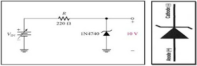
The basic function of a Zener Diode is to maintain a specific voltage across it's terminals within given limit of line or load change. Typically it is used for providing a stable reference voltage for use in power supply and other equipment.
Use of Zener Diode
- These are widely used in the voltage references and as shunt regulator to regulate the voltage across small circuit.
- These are used in the surge protectors to limit the transient voltage spikes.
Construction of Zener Diode
Zener diodes are designed to operate in reverse breakdown. There are 2 types of diodes, works well in reverse breakdown conditions "avalanche diode and zener diode". The avalanche breakdown occurs in both rectifier and zener diodes at sufficiently high reverse voltage. Low voltage causes the zener breakdown.It is heavily smear to lower the breakdown voltage. Caused a thin depletion region. These diodes breakdown characteristics are determined by the doping process. They are available with voltage breakdown of 1.8V to 200V.
Zener Breakdown Examples.
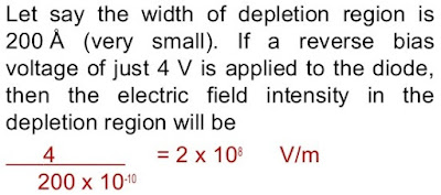
Let's say the width of depletion region is 200A (very small). If a reverse bias voltage of just 4V is applied to the diode so the intensity of the electric field will be.
Difference between Zener and Avalanche Breakdown
Zener Breakdown
- This occurs between PN junctions which is heavily doped, have narrow(small) depletion layer.
- If P and N side are good conductors then chances of high electric field exists across the depletion layer.
- If reverse applied voltage is gradually increased after a certain voltage. Here electric field is intense enough to pull electrons from the covalent bonds directly inside the depletion layer and creates current.
- As a result reverse barrier of the diode is broken down this type of breakdown is called zener breakdown.
- The voltage at this breakdown occurs is called zener breakdown voltage. You can called it Zener voltage.
Avalanche Breakdown
- A p-type semiconductor material in contact with n-type semiconductor material, forms a PN junction. in which depletion region occurs around the plane of contact.
- The depletion region may vary depending on bias applied at the terminals of the PN junction the applied voltage increase the depletion region width for the case of reverse bias.
- At reverse bias condition very little current flow through carriers this tiny current is called reverse saturation current.
- Here electric field is not strong enough to produce zener breakdown.
- Here minority collide with semi conductor atom in the depletion region, which breaks the covalent bonds and electron-holes pairs are generated. Charged carriers which are newly generated are accelerated by the electric field which results in more collision and produced avalanche of charge carriers. Avalanche breakdown occurs.
- Avalanche diodes exhibits positive temp: coefficient i.e. breakdown voltage (increases) directly proportional to temperature(increases).
What is Reverse Saturation Current:
Reverse saturation current ultimately causes the avalanche breakdown. At normal room temperature there are some semiconductor atoms which absorb sufficient energy from the heat of atmosphere to release valence electron as free electrons and create hole behind them.Moreover there is always a p-type impurity in n-type semiconductor and some n-type impurity in p-type semiconductor because of the some unwanted holes will always be present in n-type semiconductor and similarly some unwanted free electrons will be present in p-type semiconductor hence due to these unwanted impurities and also due to thermal effect of room temperature there will be some holes in present n-type site and some free electrons are present in p-type side of the PN junction.
Avalanche Breakdown.View Video.


0 Comments
Please add nice comments or answer ....